806 High Current Fuses
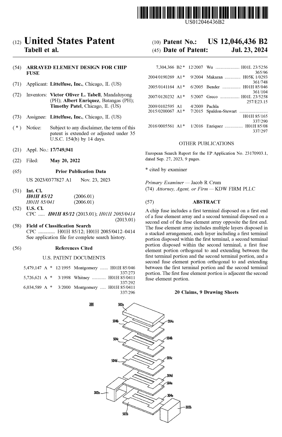
Pushing through an unsolvable fuse design constraint and earning a patent for an arrayed element architecture that brought 20-30A, high-i2t protection to the 1206 footprint for the first time.

PROJECT DETAILS
Scope
New product series · Global
Timeline
2021-2022
Location
Philippines
Program/s
Thin-Film Chip Fuse Platform
01 CONTEXT & ROLE
A customer brief with no off-the-shelf answer — and a design constraint that required new thinking
The 806 Series began with a brief from two major OEMs — Lenovo for laptops and Milwaukee for power tools — each requiring fuse protection at 20-30A in the 1206 SMD footprint at 24-36VDC, with i2t values substantially higher than anything available at that rating.
As the responsible design engineer, I led the element architecture development from initial analysis through the arrayed element concept, prototype testing, qualification, and production launch. The series remains in production today, contributing to Littelfuse's passive components business unit.
WHY THESE CUSTOMERS, WHY NOW Laptop voltage regulator modules (VRMs) and high-power cordless tool batteries were moving to higher-current architectures — demanding fuses that could handle 10x inrush at startup without nuisance blowing, within space-constrained 1206 footprints. The market gap was real, and no existing Littelfuse series could fill it. |
02 PROBLEM DEFINITION — THE WHY
The fundamental tension in fuse design — and why it could not be resolved conventionally
In fuse design, breaking capacity and i2t exist in an inverse relationship. Solving one conventionally makes the other worse — and the 806 brief required both solved simultaneously within a fixed footprint.
Requirement | Standard approach | The problem |
20-30A in 1206 footprint | Thicker element to carry higher current | Thick element in small ceramic = poor interrupting performance at 24-36VDC |
High i2t to survive 10x inrush | Increase element cross-section to raise i2t | Larger cross-section further degrades breaking capacity — the inverse tightens |
Safe interruption at 24-36VDC | Thin element to interrupt cleanly | Thinning to fix interruption reduces i2t — back to square one |
Existing designs could not be interpolated to reach the target specifications. The brief required a fundamentally different approach to fuse element architecture — one that decoupled element thickness from i2t performance.
03 DISCOVERY & RESEARCH
Finding the design space — and the analogy that unlocked the solution
Discovery began with a systematic analysis of existing thin-film element designs, mapping how element geometry, material properties, i2t, and breaking capacity related across the 1206 family.
Element geometry mapping. Modelled how element thickness, width, and material composition affected both i2t and interrupting performance. Confirmed that no single-element geometry could satisfy both requirements simultaneously — the constraint was physics, not tooling.
Failure mode analysis. Analysed how existing 1206 fuses failed under short-circuit at 24-36VDC — specifically the arc energy released when a thick element opens in a small ceramic enclosure. This established the maximum safe element mass.
The capacitor analogy. Reviewed MLCC architecture — where multiple thin dielectric layers stack in series to achieve higher voltage in a fixed footprint. This was the structural analogy that led directly to the arrayed element concept.
Material selection. Evaluated thin-film element materials and deposition processes for the arrayed architecture — balancing resistivity, thermal properties, and compatibility with existing production infrastructure.
THE INSIGHT Capacitors achieve high voltage in a small package by multiplying layers — each layer thin, the stack providing cumulative capability. What if fuse elements could do the equivalent? Not one thick element, but many thin elements in parallel, arrayed across multiple layers. |

04 SOLUTION & STRATEGIC APPROACH
The arrayed element concept — a patented architecture that resolves the inverse relationship
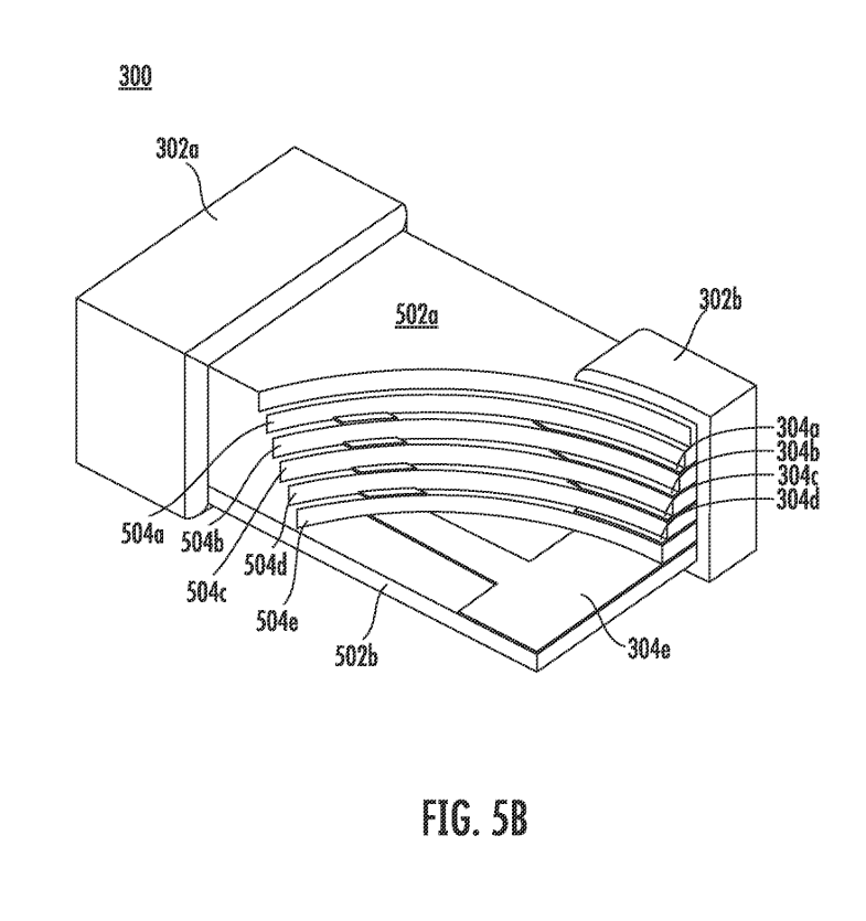
The arrayed element architecture places multiple thin elements in parallel within a single layer, then stacks multiple layers to form a three-dimensional array within the 1206 ceramic body.
Thin individual elements interrupt cleanly at high voltage — no excess arc energy, no enclosure rupture. The parallel array restores current-carrying capacity. The layered stack increases i2t without requiring any individual element to be thicker. All three customer requirements are satisfied simultaneously.
Parameter | 806 Series spec | Significance |
Current rating | 20A - 30A | High-current range in 1206 footprint — first of its kind |
Voltage rating | 24 - 36VDC | Covers laptop VRM and power tool battery architectures |
Footprint | 1206 (3.2 x 1.6mm) | Industry-standard SMD — no PCB redesign required |
i2t | High — per Littelfuse ceramic family | Withstands 10x rated inrush current at startup |
Operating temp | -55C to +150C | Suitable for elevated-temperature environments |
Compliance | UL/CSA/NMX 248-1/248-14, RoHS | Full regulatory clearance for consumer electronics and tools |

05 EXECUTION & ITERATION
From concept to patent to production — qualifying a novel architecture
Translating the arrayed element concept into a manufacturable, qualifiable product required iteration across element geometry, layer count, material deposition, and encapsulation — all within 1206 ceramic body constraints.
Element geometry optimisation. Iterated thin-film element dimensions across multiple deposition runs — balancing resistivity, i2t per element, and arc energy during interruption. Individual element mass had to stay within the safe interruption envelope for the ceramic enclosure.
Layer count and array configuration. Determined the optimal combination of elements per layer and number of layers to hit target i2t while maintaining manufacturing yield. Too many elements per layer risked positional tolerances; too few required elements too thick to interrupt safely.
Short-circuit qualification testing. Testing at 24V and 36VDC confirmed clean interruption without enclosure failure across the full current range. A fuse that fails to interrupt is a safety hazard — this was the non-negotiable gate.
Patent filing. The arrayed element architecture was novel enough that Littelfuse filed during development. The grant was awarded, protecting the architecture commercially and validating the inventive step in the design.
Customer qualification. The 806 Series passed qualification with both Lenovo and Milwaukee before mass production approval — validating the architecture's applicability across both laptop VRM and power tool battery environments.
MANUFACTURING COMPATIBILITY The arrayed element architecture had to be manufacturable within Littelfuse's existing thin-film deposition and encapsulation infrastructure — no new capital equipment. The solution had to be novel in design, not in process. That constraint shaped every geometry decision throughout development. |
06 RESULTS & IMPACT
A patent, two anchor customers, and a series still in production
The 806 Series addressed a genuine market gap — 20-30A ratings in a 1206 footprint with high i2t for VRM and power tool applications simply did not exist before this work. The product entered production, fulfilled Lenovo and Milwaukee's qualification requirements, and has continued contributing to Littelfuse's passive components revenue since launch.
The series is designed to provide overcurrent protection in circuits operating under high working ambient temperatures up to 150C, with high i2t values specifically suited to high-current voltage regulator module applications.
PERSONAL IMPACT The 806 Series taught me that the most valuable engineering contribution is recognizing when the design space has no conventional answer and developing a new approach from first principles. The habit of reasoning from analogies across domains — capacitor architecture to fuse design — is something I have brought to every product challenge since. |
WHAT I'D DO DIFFERENTLY The arrayed element concept emerged from studying an adjacent technology rather than from within the fuse design literature. A broader cross-domain research phase earlier in discovery would have surfaced this analogy sooner -- and could be a structured part of any brief that presents a genuine physics constraint. | WHAT I'D REPLICATE Filing for patent protection during active development -- before public disclosure through customer qualification -- was the right call. For any genuinely novel design approach, patent timing relative to disclosure milestones should be an early programme decision, not an afterthought. |